Haven’t gone out to get an oven toaster yet, so assembly of the first prototype board will have to wait until next weekend. Meanwhile here’s an update of what’s been done so far.

The Circuit Layout: This layout took several after-work nights, to learn how to use Cadsoft EAGLE. While the program isn’t free except for non-commercial, hobbyist use, I’ll probably buy the package shortly before I go and try build these things for sale. I’ve spent three weeks learning to place components and use the routing rules, taking the terse Allegro datasheet and application notes on the A3977 to create this circuit. The driver chip is rated at up to 35V, 2.5A, and I’ve chosen part ratings to use this with up to 24V for the motor supply. (I’ll publish the circuit diagram this following weekend, after I’ve cleaned it up a bit, as I’d been placing components haphazardly).
One of the tricky bits was ensuring that I avoid use of vias (conductive, plated-through holes that create an electrical and thermal bridge between two sides of the board) that the EAGLE autorouter insisted on placing close to (or underneath) my components. Another was to ensure hand-solderability of pin headers sans plated through holes. I also wanted the high-current motor and supply lines to lie on just one or the other side of the board; this was accomplished with those thick traces, as seen below, by disallowing any automatic vias by setting Autorouter Setup > Maximum > Via to 0 for Follow-Me, Busses and Route rulesets.
You can also force the autorouter to behave: Those odd-looking, short, rectangular “orphans” force the autorouter to go around them. After several hours experimentation spread over three nights, I figured out how to use these two tricks, plus the addition of through-hole pads (they’re a component called WIREPADs, with various inner and outer diameters) to force the motor driver lines to route underneath the PCB, where they terminate in screw terminal blocks. The same trick applied to routing of the 12-pin header that connects to my Arduino.
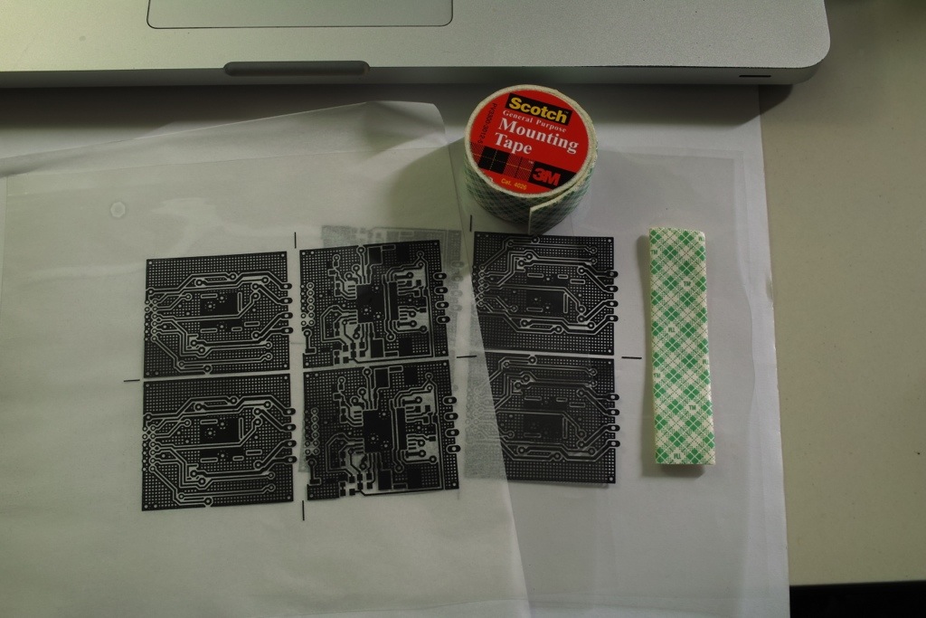
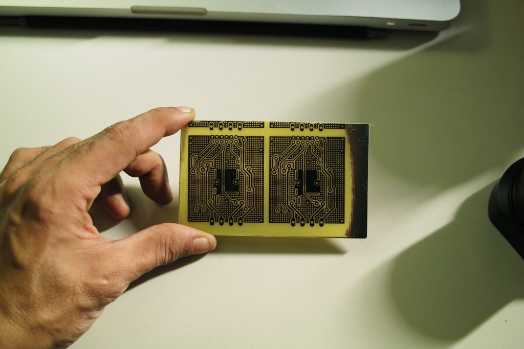
Printing the positive circuit image. I’m using presensitized copper-clad FR4 board that requires a positive exposure image (where inked areas result in copper being retained after etching), and here you’re seeing the first attempt to create four boards on my one remaining piece of 90 x 103mm blank, cut for my earlier attempt to create an Arduino prototyping shield. (That did not end well, as I’d realized that I’d need to hand-drill each of those holes and plate them through. Hence, this project).
The trick to aligning both sides begins by printing the top and bottom images from EAGLE to PostScript, first. You print the image of the top in solid black, but reversed, so that when you print it on transparency film, the fused toner is in direct contact with the PCB during exposure. If you’re creating a 4-up layout like this one, use your favorite image editor to draw ruler guide lines through plated-through holes, taking care to align two adjacent images perfectly. Do the same for the bottom side of the board, which should be printed non-reversed, as the fused toner must also be in contact with the photoemulsion. Then, duplicate the top and bottom images and group them so that you do not lose alignment between two adjacent images. Avoid using two separate sheets of transparency film by copy & pasting, or simply duplicating, the top group across the other half of the page, as shown in the next image.
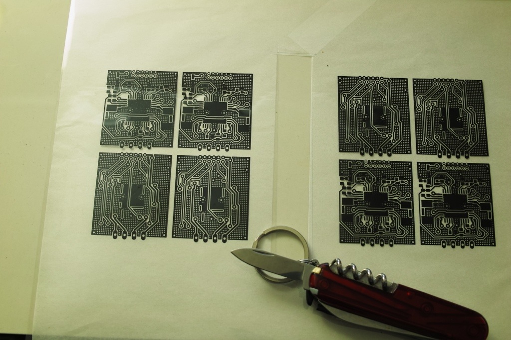
Cobble together the exposure sandwich. Now we’ve printed out the transparency containing the front and back sides of the board, on the left and right sides of a single sheet of transparency film. You’ll then fold the sheet in half to align the images. I’ve cut a rectangular hole in the transparency to ease sliding and aligning the halves of the sheet. Thick transparency films have a surprising springiness to them that impedes alignment; this cut reduces the sheet’s spring force, so that the two halves of the page don’t tend to swing/slide apart as easily. You then use double-sided tape to join the aligned sides. I use a single strip of thinner tape to bind aligned edges; then I use the thicker gauge tape to form a “pocket” into which to slide the PCB blank. You can then cut away the springy beams, as shown below.

Use your funky lightbox. This much abused piece of furniture, my desk, now also contains a lightbox that I’ve cut out using a Black and Decker router. The recessed well is an aluminum project box, that holds four 8W black light lamps. It’s a horrendously ugly piece of work that does the job. A pair of National Bookstore picture frame cover glass sheets serve as the exposure window. Our sandwich goes between those plates which, at this distance (roughly 3/5th of an inch from the tubes to the bottom sheet) requires a little under 60 seconds to fully expose the photoemulsion. We’re then ready to go to our two liquid baths.
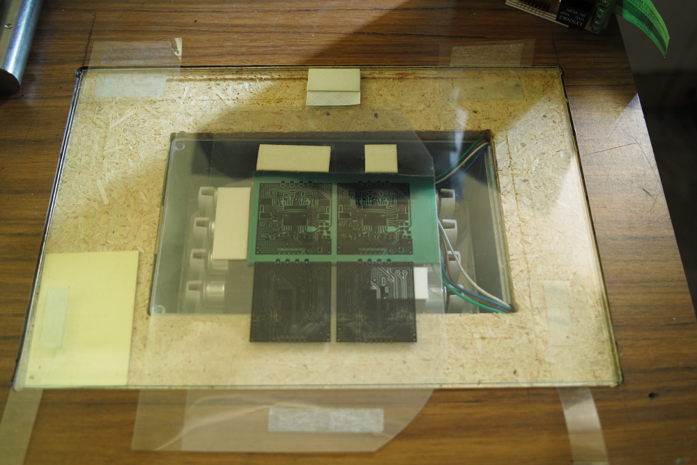
Cutting emulsion. Make sure that the fused toner on your transparency film has direct physical contact with the photoemulsion, by placing a uniform weight on the top glass before turning on the lamps. Failing to do so will result in uneven line widths or loss of some detail in the exposed emulsion. Eventually we’ll have to make an exposure frame to expose both sides simultaneously, as it is unnecessarily tedious to align and fix the film by hand. This will require printing registration marks on the film that we can align to the frame halves, an additional set of UV bulbs, and a precise hinge to hold the exposure frame together.
The exposed areas of photoemulsion are etched back by a basic solution of [what seems to be] sodium hydroxide. The little foldout instructions that come with the Alexan-branded board call it “developer”, but it’s not developer that works in the way that silver halide film works. It simply dissolves emulsion that hasn’t been photocured, and a dilute solution of drain cleaner works just as well (A 3:1 solution by volume of Liquid Sosa does the trick). This small container is dark green from having been used for that Arduino protoshield, as well as another botched attempt at this revision 1 board.

Woopsie. Notice the remaining green haze at the edge of the board: That’s a sign that this lightbox doesn’t provide uniform UV intensity across the window. I should take care to center the “sandwich” between the cathode ends of the short tubes I’m using.
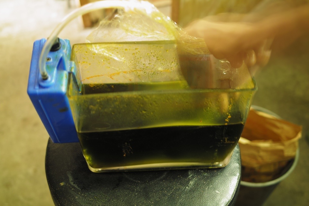
Cutting copper. I’ve repurposed this cheap glass vase as an etching tank, using a battery-powered aquarium pump as an aerator, to agitate the solution. This tank holds roughly a liter and a half of water, into which dissolves 200g of solid hydrated ferric chloride. I stir the solution with our board, with the aerator running, to ensure even etchback. If you just leave the board to rest under the stream of bubbles, the etching action works fastest where the air bubbles impinge on the board. This can lead to undercutting, where the solution cuts into the copper underneath long, thin edges of emulsion.
Wash and dry. This is the product of about an hour’s preparation and actual etching. Notice that underexposed area at the right? That’s copper overlaid with a thin coating of unexposed photoemulsion. That doesn’t pose any problems, as we’ll be cutting those edges of the board away later.
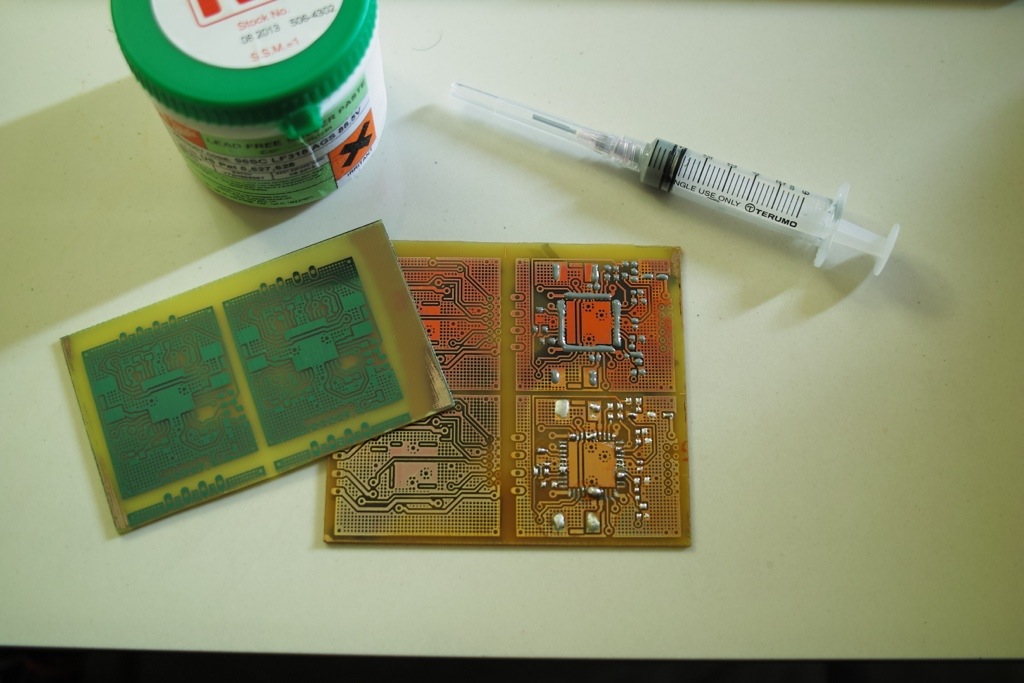
Learn yer solder paste. Now I’m using the product of my first, failed exposure attempt to find out how this solder paste behaves. The lower right quadrant of the board contains a sample of pads where I’d dabbed solder paste by hand, using a toothpick. This gives me a fair idea of how much of a change in volume to expect when I finally toast my first board using live components (solder paste volume decreases to about half, to form the final bond pad blob). Notice that the experiment board has gone light brown, where our unbaked board is a light avocado green. These are cut from the same material, except that the toasted board has been run through a couple of electric toasters.
Notice the reddish patina on the copper in the second test area – that’s the result of the 4-minute bake to create the tin-silver-copper solder beads below. This reminds me to buy a baking thermometer, and to try figure out how to ramp the temperature on a toaster by hand. I’ll get one of these cheap, two-heater toasters that will allow me to switch the heaters independently, perhaps modify it with a blower fan to eliminate hot spots.
The gray goop on the pads (upper right quadrant) is our solder paste applied with a modified syringe, which I’d then heated with a hair dryer. I’d just found out about an hour ago that this no-clean flux solder I’m using probably won’t adhere to the oxidized copper at all. After I post this, I’ll experiment with varying amounts of paste on the remaining six quadrants (four more on the backside), to get a feel for the amount of paste we’ll need to use with these surface mount components.